
Choosing an Fpga Integrated Circuit in 2026 requires more than comparing logic-cell counts. The right device must match the workload, board design, software flow, and product lifetime. A practical decision begins with the signals entering the board. Count high-speed lanes, memory interfaces, analog connections, and timing-sensitive outputs. Then examine logic elements, DSP blocks, embedded memory, I/O standards, and transceiver capability. More resources do not automatically create better performance.
Ross Freeman, the Xilinx co-founder widely recognized as the FPGA inventor, described the concept as “a blank slate.” That idea still matters. An FPGA can adapt when an algorithm changes, but flexibility demands engineering discipline. Review the vendor’s development tools, intellectual-property libraries, verification support, documentation, and device roadmap. Check whether the package fits your thermal and routing limits. A powerful chip may fail if its pins create an impossible escape pattern.
Power deserves physical attention. Imagine the regulator, heat spreader, and airflow beside the actual board, not inside a marketing diagram. Compare static power, dynamic power, clocking options, and realistic utilization. Security also requires careful review, including secure boot, bitstream protection, and supply-chain traceability. A lifecycle commitment matters for industrial, medical, and infrastructure products.
There is no perfect shortlist. A neat specification table can still mislead. Early prototypes may hide timing congestion, tool instability, or unavailable components. Leave margin. Test a representative design before committing to volume production. The best Fpga Integrated Circuit is not necessarily the largest or newest device. It is the one your team can verify, cool, source, and maintain with confidence.
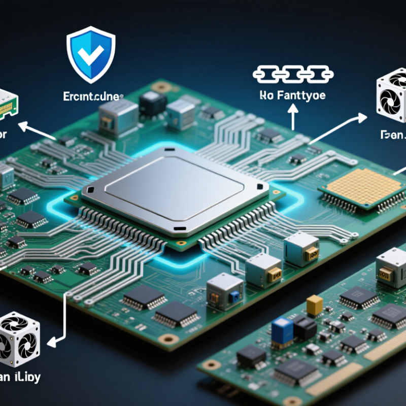
How to Choose an FPGA Integrated Circuit in 2026?
Workload definition should come before package selection. The Spring 2025 forecast from World Semiconductor Trade Statistics values global semiconductor sales at 697 billion dollars for 2025, up 11.2%. That growth reflects heavier computing and memory demands. Your design still needs measurable limits.
Count logic cells for control paths, state machines, and parallel arithmetic. Then estimate DSP blocks from actual operations per clock. A video pipeline may need one multiplier per pixel lane. A motor-control design may need fewer DSP blocks but stricter timing. BRAM capacity must cover buffers, coefficients, and dual-port access. A useful estimate is buffer depth multiplied by word width, then increased by 20% for overhead. I/O counts require more than pin totals. Check voltage banks, differential pairs, serial links, and simultaneous switching limits. The 2024 JEDEC memory standards show how higher bandwidth increases signal-integrity pressure. More pins can create more problems.
Tips: Build a simple resource spreadsheet. Record used and available logic cells, DSP blocks, BRAM, and I/O. Add 25% logic headroom and 30% memory headroom. These figures are practical starting points, not laws. Early estimates are often wrong. I once undercounted temporary line buffers because the algorithm diagram hid them. Recheck widths, clock domains, and worst-case packet sizes before choosing the device. A smaller part may reduce cost, but routing congestion can erase that advantage.
| Workload Profile | Typical Applications | Logic Cells (Approximate) | DSP Blocks (Approximate) | Block RAM (Approximate) | Available User I/O (Approximate) | Recommended Memory Capability | Design Considerations |
|---|---|---|---|---|---|---|---|
| Entry-Level Control | Simple motor control, sensor interfacing, GPIO expansion, low-speed industrial logic | 2,000–15,000 | 0–40 | 50–500 Kb | 20–120 | Small on-chip buffers; external memory usually unnecessary | Prioritize low power, compact packaging, sufficient voltage standards, and predictable I/O timing. |
| General-Purpose Embedded Processing | Protocol bridging, embedded CPUs, machine control, industrial communications, moderate data acquisition | 15,000–60,000 | 40–200 | 0.5–4 Mb | 80–300 | On-chip RAM plus optional external DDR memory | Allow additional logic for soft processors, bus interconnects, DMA engines, and peripheral controllers. |
| Digital Signal Processing | Audio processing, software-defined radio, radar preprocessing, vibration analysis, image filtering | 30,000–150,000 | 150–1,000 | 2–16 Mb | 150–500 | High-bandwidth external DDR memory is often beneficial | Estimate multiplier width, samples per clock, filter taps, clock frequency, and the number of parallel pipelines. |
| High-Speed Networking | Packet processing, network appliances, time-sensitive networking, data aggregation, communications infrastructure | 80,000–300,000 | 200–1,500 | 8–40 Mb | 300–900 | Multiple external memory channels may be required | Check transceiver count, line rate, packet-buffer capacity, MAC support, and latency requirements in addition to I/O count. |
| Video and Imaging | Multi-camera capture, display pipelines, computer vision preprocessing, image scaling and enhancement | 100,000–500,000 | 300–2,000 | 16–80 Mb | 300–1,000 | External DDR memory is normally required for frame buffers | Calculate memory bandwidth from resolution, frame rate, pixel format, buffering depth, and the number of video streams. |
| Compute-Intensive AI Inference | Edge classification, object detection, signal classification, industrial machine vision | 150,000–800,000 | 500–4,000 | 32–160 Mb | 400–1,200 | High-bandwidth memory subsystem and/or external accelerator memory | Evaluate arithmetic precision, accumulated operations per second, model size, tensor reuse, and memory movement overhead. |
| Large-Scale System Integration | Multi-channel instrumentation, hardware acceleration, complex communications, large industrial platforms | 300,000–1,500,000+ | 1,000–6,000+ | 64–500 Mb | 600–2,000+ | High-capacity external memory, advanced interconnects, and multiple clock domains | Reserve at least 20–30% capacity for routing, timing closure, software changes, and future feature expansion. |
Planning note: The ranges above are technology-independent engineering estimates rather than specifications for a particular device. Actual utilization depends on logic architecture, RAM granularity, DSP configuration, package options, I/O voltage standards, routing congestion, clocking, and implementation constraints. For reliable selection, target no more than approximately 70–80% utilization after synthesis and place-and-route.

© 2024 Sierramotion. All Rights Reserved